E-Beam Atomic-scale 3-D ‘Sculpting’ Could Enable New Quantum Nanodevices
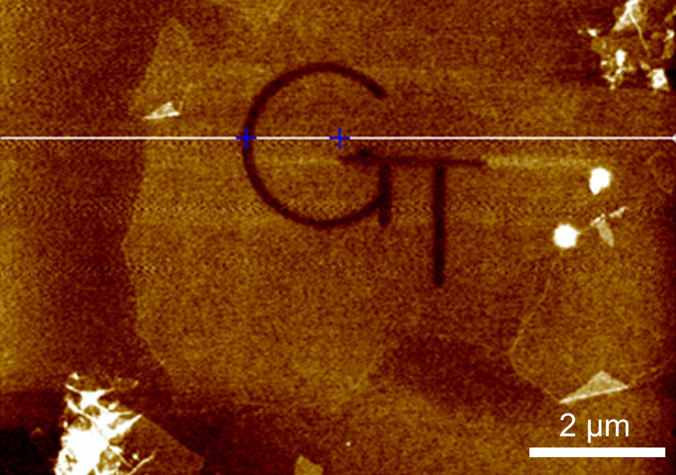
Image shows patterned etching of graphene oxide flakes to create a logo. The etching achieved a depth of 0.9 nanometers.
By varying the energy and dose of tightly focused electron beams, researchers have demonstrated the ability to both etch away and deposit high-resolution nanoscale patterns on two-dimensional layers of graphene oxide. The 3D additive/subtractive “sculpting” can be done without changing the chemistry of the electron beam deposition chamber, providing the foundation for building a new generation of nanoscale structures.
Based on focused electron beam-induced processing (FEBID) techniques, the work could allow production of 2D/3D complex nanostructures and functional nanodevices useful in quantum communications, sensing, and other applications. For oxygen-containing materials such as graphene oxide, etching can be done without introducing outside materials, using oxygen from the substrate.
“By timing and tuning the energy of the electron beam, we can activate interaction of the beam with oxygen in the graphene oxide to do etching, or interaction with hydrocarbons on the surface to create carbon deposition,” said Andrei Fedorov, professor and Rae S. and Frank H. Neely Chair in the George W. Woodruff School of Mechanical Engineering at the Georgia Institute of Technology. “With atomic-scale control, we can produce complicated patterns using direct write-remove processes. Quantum systems require precise control on an atomic scale, and this could enable a host of potential applications.”
The technique was described August 7 in the journal ACS Applied Materials & Interfaces. The work was supported by the U.S. Department of Energy Office of Science, Basic Energy Sciences. Coauthors included researchers from Pusan National University in South Korea.
Creation of nanoscale structures is traditionally done using a multistep process of photoresist coating and patterning by photo- or electron beam lithography, followed by bulk dry/wet etching or deposition. Use of this process limits the range of functionalities and structural topologies that can be achieved, increases the complexity and cost, and risks contamination from the multiple chemical steps, creating barriers to fabrication of new types of devices from sensitive 2D materials.
FEBIP enables a material chemistry/site-specific, high-resolution multimode atomic scale processing and provides unprecedented opportunities for “direct-write,” single-step surface patterning of 2D nanomaterials with an in-situ imaging capability. It allows for realizing a rapid multiscale/multimode “top-down and bottom-up” approach, ranging from an atomic scale manipulation to a large-area surface modification on nano- and microscales.
“By tuning the time and the energy of the electrons, you can either remove material or add material,” Fedorov said. “We did not expect that upon electron exposure of graphene oxide we would start etching patterns.”
With graphene oxide, the electron beam introduces atomic scale perturbations into the 2D-arranged carbon atoms and uses embedded oxygen as an etchant to remove carbon atoms in precise patterns without introduction of a material into the reaction chamber. Fedorov said any oxygen-containing material might produce the same effect. “It’s like the graphene oxide carries its own etchant,” he said. “All we need to activate it is to ‘seed’ the reaction with electrons of appropriate energy.”
For adding carbon, keeping the electron beam focused on the same spot for a longer time generates an excess of lower-energy electrons by interactions of the beam with the substrate to decompose the hydrocarbon molecules onto the surface of the graphene oxide. In that case, the electrons interact with the hydrocarbons rather than the graphene and oxygen atoms, leaving behind liberated carbon atoms as a 3D deposit.
“Depending on how many electrons you bring to it, you can grow structures of different heights away from the etched grooves or from the two-dimensional plane,” he said. “You can think of it almost like holographic writing with excited electrons, substrate and adsorbed molecules combined at the right time and the right place.”
The process should be suitable for depositing materials such as metals and semiconductors, though precursors would need to be added to the chamber for their creation. The 3D structures, just nanometers high, could serve as spacers between layers of graphene or as active sensing elements or other devices on the layers.
“If you want to use graphene or graphene oxide for quantum mechanical devices, you should be able to position layers of material with a separation on the scale of individual carbon atoms,” Fedorov said. “The process could also be used with other materials.”
Using the technique, high-energy electron beams can produce feature sizes just a few nanometers wide. Trenches etched in surfaces could be filled with metals by introducing metal atoms containing precursors.
Beyond simple patterns, the process could also be used to grow complex structures. “In principle, you could grow a structure like a nanoscale Eiffel Tower with all the intricate details,” Fedorov said. “It would take a long time, but this is the level of control that is possible with electron beam writing.”
Though systems have been built to use multiple electron beams in parallel, Fedorov doesn’t see them being used in high-volume applications. More likely, he said, is laboratory use to fabricate unique structures useful for research purposes.
“We are demonstrating structures that would otherwise be impossible to produce,” he said. “We want to enable the exploitation of new capabilities in areas such as quantum devices. This technique could be an imagination enabler for interesting new physics coming our way with graphene and other interesting materials.”
In addition to Fedorov, the research team included Songkil Kim, SungYeb Jung, Jaekwang Lee, and Seokjun Kim from Pusan National University in South Korea.
This research was supported primarily by the U.S. Department of Energy, Office of Science, Basic Energy Sciences, under award no. DE-SC0010729, and by the National Research Foundation of Korea grant MSIT no. 2019R1C1C1010556 funded by the Korean government. Any opinions, findings, and conclusions or recommendations expressed in this material are those of the authors and do not necessarily reflect the views of the sponsoring organizations.
CITATION: Songkil Kim, et al., “High-Resolution Three-Dimensional Sculpting of Two-Dimensional Graphene Oxide by E‑Beam Direct Write.” (ACS Applied Materials & Interface, 2020.) https://doi.org/10.1021/acsami.0c11053